

OEM PCB Fabrication Prototype from Top China Manufacturer for Custom Solutions
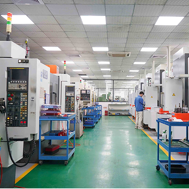
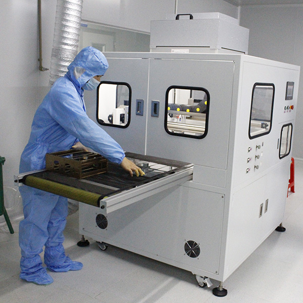
When I think about OEM PCB fabrication prototypes, I picture precision and reliability that meet my specific needs. As a leading manufacturer in China, we understand the importance of prototyping in bringing innovative electronic designs to life. Our services are tailored to help businesses like yours achieve rapid development cycles without compromising on quality. With state-of-the-art technology and a commitment to excellence, I ensure that each PCB prototype is crafted with exceptional care. Whether you're in the early stages of development or ready for mass production, our team is here to support you every step of the way. Plus, working directly with us means faster communication and a more personalized experience. If you're seeking a trusted partner for your OEM PCB fabrication prototype needs, I’m excited to offer you solutions that can help propel your projects forward. Let's collaborate to turn your ideas into reality, efficiently and effectively!
OEM Pcb Fabrication Prototype Where Innovation Meets 2025 Your Trusted OEM Partner
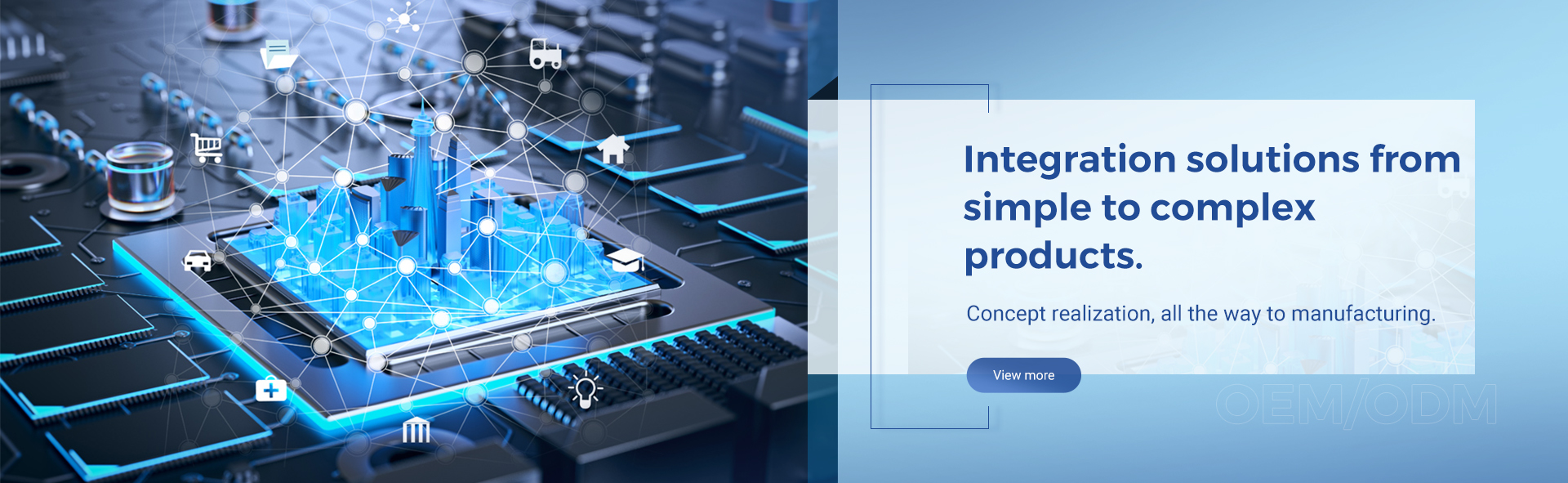
In the fast-evolving realm of electronics, the demand for high-quality, precise printed circuit board (PCB) fabrication is ever-increasing. As we approach 2025, the convergence of technological innovation and manufacturing capabilities is redefining the standards for OEM partnerships. For global buyers seeking reliable and capable partners, having access to advanced prototyping services is crucial. Our dedicated approach to PCB fabrication emphasizes quality and innovation, offering prototypes that meet stringent industry standards while enabling rapid development cycles. By leveraging state-of-the-art technology and a skilled workforce, we ensure that your ideas are translated into tangible, functional designs quickly and efficiently. Whether you’re in the automotive, telecommunications, or consumer electronics sectors, our tailored solutions cater to diverse application needs, ensuring that you remain competitive in the global market. Choosing the right OEM partner can significantly impact your product development lifecycle. With a commitment to excellence and an unwavering focus on customer satisfaction, we position ourselves as your trusted ally in navigating the complexities of PCB fabrication. Together, we can transform your concepts into reality, driving forward the innovations that will shape the future of technology.
OEM Pcb Fabrication Prototype Where Innovation Meets 2025 Your Trusted OEM Partner
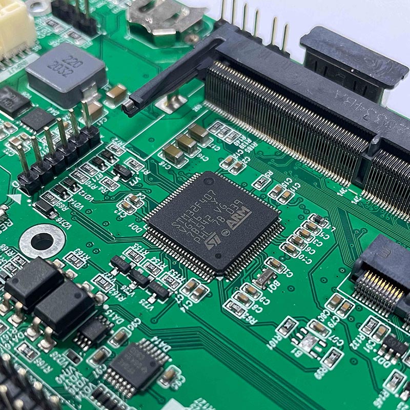
| Parameter | Description | Value |
|---|---|---|
| Layer Count | Number of PCB layers | 4 |
| Material Type | Core material of PCB | FR-4 |
| Copper Thickness | Thickness of copper layers | 1 oz |
| Board Thickness | Overall thickness of PCB | 1.6 mm |
| Surface Finish | Finish applied to PCB surface | HASL |
| Minimum Trace Width | Narrowest width of a trace | 0.2 mm |
| Minimum Hole Size | Smallest diameter of a hole | 0.3 mm |
| Prototype Turnaround Time | Time to complete prototype | 5-7 days |
Related Products

OEM Pcb Fabrication Prototype Your Trusted OEM Partner Service Backed by Expertise
Top Selling Products
- Related Blog
- Reviews
- Reviews
