


EMS solutions for Printed Circuit Board
Description
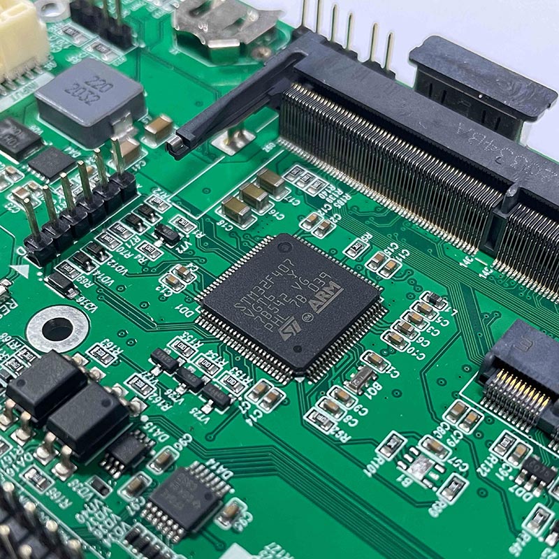
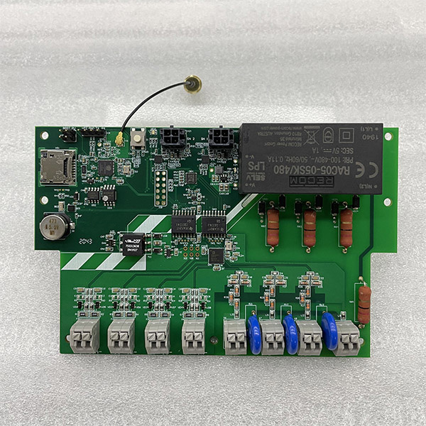
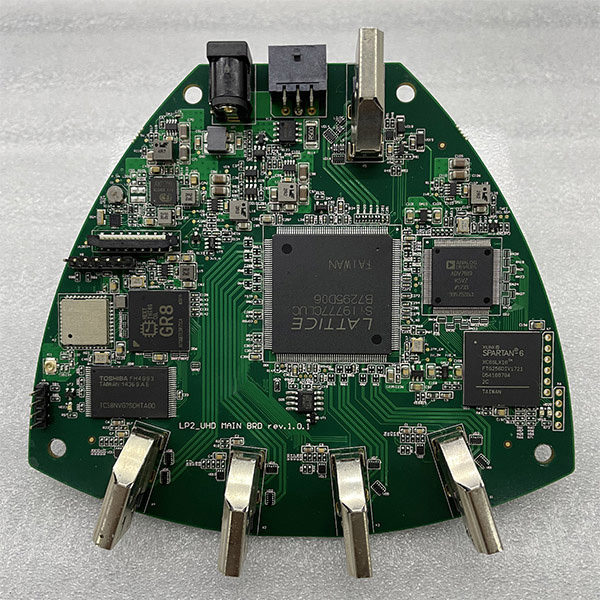
Equipped with SPI, AOI, and X-ray device for 20 SMT lines, 8 DIP, and test lines, we offer an advanced service that includes a wide range of assembly techniques and produce the multi-layers PCBA, flexible PCBA. Our professional laboratory has ROHS, drop, ESD, and high & low temperature testing devices. All of the products are conveyed by strict quality control. Using the advanced MES system for manufacturing management under IAF 16949 standard, we handle the production effectively and securely.
By combining the resources and the engineers, we can also offer the program solutions, from the IC program development and software to electric circuit design. With experience in developing projects in healthcare and customer electronics, we can take over your ideas and bring the actual product to life. By developing the software, program, and the board itself, we can manage the whole manufacturing process for the board, as well as the final products. Thanks to our PCB factory and the engineers, it provides us with competitive advantages compared to the ordinary factory. Based on the product design & development team, the established manufacturing method of different quantities, and effective communication between the supply chain, we are confident of face the challenges and get the work done.
|
PCBA Capability |
|
|
Automatic equipment |
Description |
|
Laser marking machine PCB500 |
Marking range: 400*400mm |
| Speed: ≤7000mm/S | |
| Maximum power: 120W | |
| Q-switching, Duty Ratio: 0-25KHZ; 0-60% | |
|
Printing machine DSP-1008 |
PCB size: MAX:400*34mm MIN:50*50mm T:0.2~6.0mm |
| Stencil size: MAX:737*737mm MIN:420*520mm |
|
| Scraper pressure: 0.5~10Kgf/cm2 | |
| Cleaning method: Dry cleaning, wet cleaning, vacuum cleaning (programmable) | |
| Printing speed: 6~200mm/sec | |
| Printing accuracy: ±0.025mm | |
|
SPI |
Measuring principle: 3D White Light PSLM PMP |
| Measurement item: Solder paste volume, area, height, XY offset, shape | |
| Lens resolution: 18um | |
| Precision: XY resolution: 1um; High speed: 0.37um |
|
| View dimension: 40*40mm | |
| FOV speed: 0.45s/FOV | |
|
High speed SMT machine SM471 |
PCB size: MAX:460*250mm MIN:50*40mm T:0.38~4.2mm |
| Number of mounting shafts: 10 spindles x 2 cantilevers | |
| Component size: Chip 0402(01005 inch) ~ □14mm(H12mm) IC,Connector(lead pitch 0.4mm),※BGA,CSP(Tin ball spacing 0.4mm) | |
| Mounting accuracy: chip ±50um@3ó/chip, QFP ±30um@3ó/chip | |
| Mounting speed: 75000 CPH | |
|
High speed SMT machine SM482 |
PCB size: MAX:460*400mm MIN:50*40mm T:0.38~4.2mm |
| Number of mounting shafts: 10 spindles x 1 cantilever | |
| Component size: 0402(01005 inch) ~ □16mm IC,Connector(lead pitch 0.4mm),※BGA,CSP(Tin ball spacing 0.4mm) | |
| Mounting accuracy: ±50μm@μ+3σ (according to standard chip's size) | |
| Mounting speed: 28000 CPH | |
|
HELLER MARK III Nitrogen reflux furnace |
Zone: 9 heating zones, 2 cooling zones |
| Heat source: Hot air convection | |
| Temperature control precision: ±1℃ | |
| Thermal compensation capacity: ±2℃ | |
| Orbital speed: 180—1800mm/min | |
| Track width range: 50—460mm | |
|
AOI ALD-7727D |
Measuring principle: The HD camera obtains the reflection state of each part of the three-color light irradiating on the PCB board, and judges it by matching the image or logical operation of gray and RGB values of each pixel point |
| Measurement item: Solder paste printing defects, parts defects, solder joint defects | |
| Lens resolution: 10um | |
| Precision: XY resolution: ≤8um | |
|
3D X-RAY AX8200MAX |
Maximum detection size: 235mm*385mm |
| Maximum power: 8W | |
| Maximum voltage: 90KV/100KV | |
| Focus size: 5μm | |
| Safety (radiation dose): <1uSv/h | |
|
Wave soldering DS-250 |
PCB width: 50-250mm |
| PCB transmission height: 750 ± 20 mm | |
| Transmission speed: 0-2000mm | |
| Length of preheating zone: 0.8M | |
| Number of preheating zone: 2 | |
| Wave number: Dual wave | |
|
Board splitter machine |
Working range: MAX:285*340mm MIN:50*50mm |
| Cutting precision: ±0.10mm | |
| Cutting speed: 0~100mm/S | |
| Speed of rotation of spindle: MAX:40000rpm | |
|
Technology Capability |
||
|
Number |
Item |
Great capability |
|
1 |
base material | Normal Tg FR4, High Tg FR4, PTFE, Rogers, Low Dk/Df etc. |
|
2 |
Solder mask color | green, red, blue, white, yellow, purple,black |
|
3 |
Legend color | white, yellow, black, red |
|
4 |
Surface treatment type | ENIG, Immersion tin, HAF, HAF LF, OSP, flash gold, gold finger, sterling silver |
|
5 |
Max. layer-up(L) | 50 |
|
6 |
Max. unit size (mm) | 620*813 (24"*32") |
|
7 |
Max. working panel size (mm) | 620*900 (24"x35.4") |
|
8 |
Max. board thickness (mm) | 12 |
|
9 |
Min. board thickness(mm) | 0.3 |
|
10 |
Board thickness tolerance (mm) | T<1.0 mm: +/-0.10mm ; T≥1.00mm: +/-10% |
|
11 |
Registration tolerance (mm) | +/-0.10 |
|
12 |
Min. mechanical drilling hole diameter (mm) | 0.15 |
|
13 |
Min. laser drilling hole diameter(mm) | 0.075 |
|
14 |
Max. aspect(through hole) | 15:1 |
| Max. aspect(micro-via) | 1.3:1 | |
|
15 |
Min. hole edge to copper space(mm) | L≤10, 0.15;L=12-22,0.175;L=24-34, 0.2;L=36-44, 0.25;L>44, 0.3 |
|
16 |
Min. innerlay clearance(mm) | 0.15 |
|
17 |
Min. hole edge to hole edge space(mm) | 0.28 |
|
18 |
Min. hole edge to profile line space(mm) | 0.2 |
|
19 |
Min. innerlay copper to profile line sapce (mm) | 0.2 |
|
20 |
Registration tolerace between holes (mm) | ±0.05 |
|
21 |
Max. finished copper thickness(um) | Outer Layer: 420 (12oz) Inner Layer: 210 (6oz) |
|
22 |
Min. trace width (mm) | 0.075 (3mil) |
|
23 |
Min. trace space (mm) | 0.075 (3mil) |
|
24 |
Solder mask thickness (um) | line corner : >8 (0.3mil) upon copper: >10 (0.4mil) |
|
25 |
ENIG golden thickness (um) | 0.025-0.125 |
|
26 |
ENIG nickle thickness (um) | 3-9 |
|
27 |
Sterling silver thickness (um) | 0.15-0.75 |
|
28 |
Min. HAL tin thickness (um) | 0.75 |
|
29 |
Immersion tin thickness (um) | 0.8-1.2 |
|
30 |
Hard-thick gold plating gold thickness (um) | 1.27-2.0 |
|
31 |
golden finger plating gold thickness (um) | 0.025-1.51 |
|
32 |
golden finger plating nickle thickness(um) | 3-15 |
|
33 |
flash gold plating gold thickness (um) | 0,025-0.05 |
|
34 |
flash gold plating nickle thickness (um) | 3-15 |
|
35 |
profile size tolerance (mm) | ±0.08 |
|
36 |
Max. solder mask plugging hole size (mm) | 0.7 |
|
37 |
BGA pad (mm) | ≥0.25 (HAL or HAL Free:0.35) |
|
38 |
V-CUT blade position tolerance (mm) | +/-0.10 |
|
39 |
V-CUT position tolerance (mm) | +/-0.10 |
|
40 |
Gold finger bevel angle tolerance (o) | +/-5 |
|
41 |
Impedence tolerance (%) | +/-5% |
|
42 |
Warpage tolerance (%) | 0.75% |
|
43 |
Min. legend width (mm) | 0.1 |
|
44 |
Fire flame calss | 94V-0 |
|
Special for Via in pad products |
Resin plugged hole size (min.) (mm) | 0.3 |
| Resin plugged hole size (max.) (mm) | 0.75 | |
| Resin plugged board thickness (min.) (mm) | 0.5 | |
| Resin plugged board thickness (max.) (mm) | 3.5 | |
| Resin plugged maximum aspect ratio | 8:1 | |
| Resin plugged minimum hole to hole space (mm) | 0.4 | |
| Can difference hole size in one board? | yes | |
|
Back plane board |
Item | |
| Max. pnl size (finished) (mm) | 580*880 | |
| Max. working panel size (mm) | 914 × 620 | |
| Max. board thickness (mm) | 12 | |
| Max. layer-up(L) | 60 | |
| Aspect | 30:1 (Min. hole: 0.4 mm) | |
| Line wide/space (mm) | 0.075/ 0.075 | |
| Back drill capability | Yes | |
| Tolerance of back drill (mm) | ±0.05 | |
| Tolerance of press fit holes (mm) | ±0.05 | |
| Surface treatment type | OSP, sterling silver, ENIG | |
|
Rigid-flex board |
Hole size (mm) | 0.2 |
| Dielectrical thickness (mm) | 0.025 | |
| Working Panel size (mm) | 350 x 500 | |
| Line wide/space (mm) | 0.075/ 0.075 | |
| Stiffener | Yes | |
| Flex board layers (L) | 8 (4plys of flex board) | |
| Rigid board layers (L) | ≥14 | |
| Surface treatment | All | |
| Flex board in mid or outer layer | Both | |
|
Special for HDI products |
Laser drilling hole size (mm) |
0.075 |
|
Max. dielectric thickness (mm) |
0.15 | |
|
Min. dielectric thickness (mm) |
0.05 | |
|
Max. aspect |
1.5:1 | |
|
Bottom Pad size (under micro-via) (mm) |
Hole size+0.15 | |
|
Top side Pad size ( on micro-via) (mm) |
Hole size+0.15 | |
|
Copper filling or not (yes or no) (mm) |
yes | |
|
Via in Pad design or not ( yes or no) |
yes | |
|
Buried hole resin plugged (yes or no) |
yes | |
|
Min. via size can be copper filled (mm) |
0.1 | |
|
Max. stack times |
any layer | |