


Expert Printed Wiring Board Design: Your ODM Supplier Solution
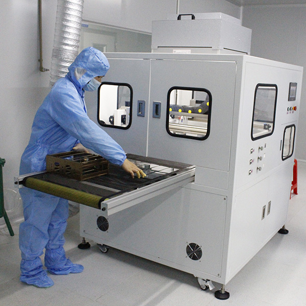
When seeking top-notch printed wiring board design, I understand the importance of having a reliable ODM supplier by your side. My experience in this field allows me to offer tailored solutions that meet the unique needs of your project. Each design is crafted with precision, ensuring optimal performance and durability. I pride myself on collaboration, working closely with clients to transform their ideas into successful products. Whether you're in the early stages of development or need revisions for existing designs, I am here to provide support every step of the way. My commitment to quality and timely delivery means you can trust that your printed wiring boards will exceed expectations. With competitive pricing and a focus on customer satisfaction, I invite you to reach out and discuss how we can bring your vision to life. Together, we can achieve outstanding results in the world of electronics!
Printed Wiring Board Design Stands Out Winning in 2025
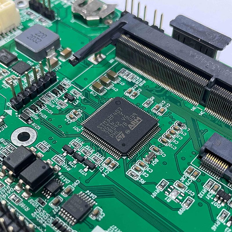
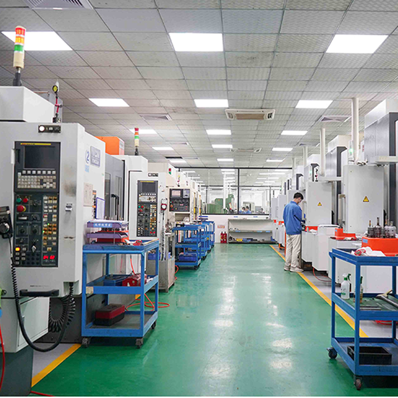
In 2025, the electronic manufacturing landscape is evolving at an unprecedented pace, and the design of printed wiring boards (PWBs) is taking center stage. As global demand for innovative electronic solutions continues to rise, the efficiency and precision of PWB design have never been more critical for businesses across various industries. A well-designed PWB can significantly enhance product reliability, reduce manufacturing costs, and accelerate time-to-market—allowing companies to stay competitive in a rapidly changing environment. The key to winning in the PWB design space lies in embracing advanced technologies and methodologies. Techniques such as 3D modeling, automated design rule checks, and simulation tools are enabling designers to create more complex and compact layouts that meet the increasing performance requirements of modern electronics. Moreover, integrating materials with superior thermal and electrical properties ensures that the final products not only perform well but also sustain longer operational lifespans. Collaboration across the supply chain is another vital factor in achieving excellence in PWB design. By engaging with suppliers, manufacturers, and end-users early in the design process, companies can better understand market needs and innovate accordingly. As businesses strive for sustainability, focusing on eco-friendly materials and designs will not only appeal to environmentally conscious consumers but also align with global regulatory trends. Adopting a holistic approach to PWB design can set companies apart and drive success in the competitive electronics marketplace of 2025 and beyond.
Printed Wiring Board Design Stands Out Winning in 2025
| Dimension | Value | Notes |
|---|---|---|
| Layer Count | 12 Layers | High-density interconnect technology |
| Board Thickness | 1.6 mm | Standard thickness for multilayer boards |
| Copper Weight | 1 oz / 2 oz | Flexible options for power requirements |
| Finish Type | ENIG | Electroless Nickel Immersion Gold for reliability |
| Max Operating Temperature | 130 °C | Designed for high-performance applications |
| Production Volume | 100,000 units/year | Scalable production to meet demand |
Related Products

Printed Wiring Board Design Leads the Global Market Delivers Unmatched Quality
Top Selling Products
- Related Blog
- Reviews
- Reviews
